Defining Innovation in Nanotech and Miniaturization


YES’s technologists are experts in modifying surfaces to encourage bonding between unlike materials. Whether through plasma bombardment, chemical reaction or a combination of the two, YES systems can help solve your adhesion problem.
YES plasma systems gently but effectively remove oxidation and contaminants from bond pads to enable strong adhesion without affecting sensitive electronics.
The ions generated by YES’s environmentally safe oxygen plasma systems bond quickly and completely with metal oxides, leaving behind clean metal surfaces with no substrate damage
In device fabrication, photoresist is used to transfer a pattern onto a substrate. Once the pattern is created in the resist, a descum operation removes trace amounts of resist and other residues. After the pattern is transferred, the remaining photoresist must be removed from the substrate before it can move to the next processing step. YES’s plasma cleaning systems are effective for stripping thick layers of photoresist, as well as descumming, etching, and removing organics.
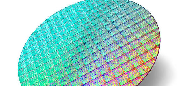
Whether the substrate is a silicon semiconductor wafer, a glass microscope slide or a plastic microfluidics device, YES cleaning systems provide thorough yet gentle plasma cleaning with no surface damage.
YES plasma systems provide gentle, predictable, tunable surface cleaning without using hazardous solvents, for contamination-free sample preparation. Glass slides, which can vary in quality from batch to batch, can be prepared with plasma for consistent surface coating. In addition, medical device materials including metals (e.g. Ti, Co-Cr) and polymers (e.g. UHMWPE, PEEK) can be properly cleaned, prepared and textured (at micro and/or macro scale) to promote strong adhesion of a broad range of coatings.
For greater control in the application of photoresist, YES coating systems can apply a reflection-blocking film that significantly improves resolution by eliminating extraneous light.
The thorough dehydration and precise monolayer coating provided by a YES vapor phase deposition system makes high contact angles possible, for optimal hydrophobicity. This hydrophobic coating reduces stiction, the undesired static friction that wears down MEMS and other nanoscale devices. Minimizing stiction improves device reliability and longevity, and prevents damaging lock-up, which can occur when the device flexes and sticks to itself.
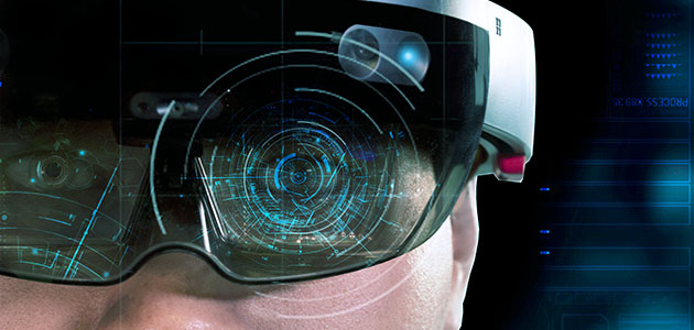
Whether you want a slick surface to glide a diffractive waveguide film from its mold or a sticky surface to ensure the adhesion of the film to glass or another substrate, YES systems enable the surface modifications needed for AR/VR and other advanced optical applications.
Performance-proven monolayer coating systems from YES enable polymers to achieve very high contact angles, creating the hydrophobicity needed to slide a liquid specimen smoothly down a single-cell-wide microfluidic channel.
YES coating systems can apply a protective passivation coat to keep sensitive electronics safe from UV, moisture, and environmental contamination.
YES systems’ controlled process environment assures consistent deposition of Self Assembled Monolayer (SAM) films. YES has experience depositing over 100 chemical precursors including alkyl, amino, epoxy, and fluorinated-silane derivatives. These may be used as the basis of attachment of additional coating layers to achieve more complex multi-layer coatings or for attachment of biomolecules such as bio-active peptides. Aminosilanes such as APTES can provide molecular-specific bonding sites for DNA and oligonucleotide adhesion in microarrays, enabling uniform and stable attachment of these and other functional biomolecules.
Benzocyclobutene (BCB) is used to create photosensitive polymers, which require fewer processing steps than dry etch materials. BCB’s primary advantage over other polymers is its compatibility with conventional integrated circuit (IC) processing techniques as well as with various metallization systems. BCB also has a low-K dielectric, a low dissipation factor at high frequencies, low moisture absorption, and a high degree of planarization. BCB-based polymer dielectrics may be spun on or applied to a variety of substrates for use in MEMS and microelectronics processing. Typical applications include adhesive wafer bonding, low-K dielectrics, CMOS, bipolar devices, optical interconnects, and intracortical neural implants. The YES-PB Series and the fully automated YES-VertaCure are ideally suited for this process.
The YES VertaCure system is well-suited to metal annealing. Annealing is a heat treatment that improves the metallic layer of a semiconducting material, changing its electrical properties, increasing grain size for faster polishing, providing better conductivity, reducing surface tension, minimizing electromigration, and allowing a consistent CMP rate across the substrate.
Trapped moisture can seriously degrade a device’s reliability. YES high-temperature curing systems rid substrates of surface moisture and chemically-bound water molecules, quickly remove airborne oxygen and water vapor from the chamber gas, and use silane vapor deposition to create long-lasting moisture-resistant surfaces.
Complete moisture removal from porous low-K material poses a major challenge to process engineers. To retain the integrity of the dielectric, YES equipment uses a series of vacuum pulls and hot nitrogen purges to ensure that the sidewalls of the pores are completely dehydrated, made hydrophobic, and sealed against further moisture incursion. In addition, YES vapor deposition systems can restore low-K dielectrics that have incurred damage from ashing.
Polyimides are high temperature polymers with excellent mechanical, thermal, and electrical properties. Typically, they are applied in liquid form and then thermally cured as a thin film or layer. YES vacuum curing systems provide thorough, uniform solvent evaporation, leaving no bubbles trapped in the polyimide film. Precise temperature control avoids cracks and color variations, and ensures complete imidization and good film adhesion. To maintain film transparency (critical for multi-layer processes), oxygen levels are kept below 10ppm during processing. The YES process module’s Class 1 environment makes use of laminar flow to eliminate particles.
Silane deposition is needed to promote the chemical adhesion of an organic compound (photoresist) to a non-organic substrate. The silane, typically hexamethyldisilizane (HMDS) acts as a sort of “bridge,” with properties that will bond to both the photoresist and wafer surface. Combining substrate dehydration and vapor deposition of HMDS, YES systems produce an HMDS prime layer with superior uniformity and stability. So-called “wet” processes for depositing silane generate a substantial amount of hazardous waste. Plus, the coating has a limited lifespan, meaning a process engineer has a small window of time to apply photoresist before the bond degrades. YES’s HMDS vapor prime process significantly extends the time available between process steps. Plus, the vapor deposition process typically uses less than 1% of the amount needed for wet application processes, significantly reducing waste and chemical costs.
Wafer Level Packaging (WLP) technology extends Moore’s Law by combining multiple elements into a low-profile, small form-factor package with excellent electrical and thermal performance. Various types of devices, packages or components are placed side-by-side and embedded with epoxy mold compound. This is followed by thin-film processing, repassivation and metallization on one or both sides of the wafer to fan out interconnections from original die pads to external pad locations. To cure the film, YES systems use a gentle vacuum process that reduces particles, shortens process time, requires less nitrogen, and eliminates discoloration, trapped solvent and outgassing at metallization.