APPLICATIONS
IMAGE REVERSAL
Image Reversal
 

This process reverses the action of positive resist so negative images can be formed with the same resolution and processing ease that a positive resist allows. What’s more, image reversal allows variations of the slope of the photoresist sidewall for higher resolution and/or lift off profiles.

For example, if the normal slope of approximately 68 degrees is altered to 90 degrees vertical, resolution is increased 20%. And, if an angle of 112 degrees is achieved, there is a strong overhang that makes metal deposition followed by liftoff controllable.

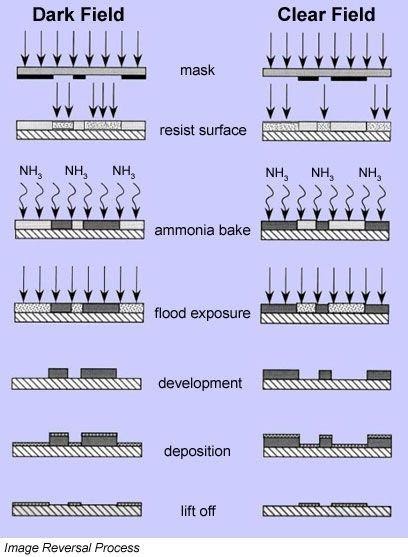
Image reversal advantages:

  • Allows variations of the slope of the photoresist sidewall for higher resolution and improved lift off. Replaces use of harsh chemicals or plasma “metal etch” processes.
  • Using image reversal on two or more layer resist levels can eliminate residual photoresist along the sidewalls, preventing “shorts” from level to level without reducing line width.
  • Image reversal done with dark or light fields eliminates standing waves; this allows steep and straight profiles, repeatable results, and excellent chemical deposition uniformity.
  • Image reversal achieves excellent results for rework problems; underlying substrate is protected (for a double metal process), so unwanted metal can be stripped away without pitting or eroding the underlying level.

Why not just use a negative resist?

Positive resist offers far better resolution, and it doesn’t require solvents for development. In contrast, the resolution limit of negative resist is approximately 1 micron, and it requires solvents known to be carcinogens.

YES image reversal systems deliver anhydrous ammonia (NH3) into a vacuum oven. There are two advantages of an ammonia system: 1) easier control of vapor pressure, and 2) an absence of residual water vapor, which will react with the NH3 to produce NH3OH, a corrosive to the system that also creates contaminating particles.

For more information on achieving repeatable and usable reversals, visit the YES-58TA & 310TA product pages.

Site Map
APPLICATIONS
PHOTORESIST TREATMENT
Photoresist Treatment

RESIST ADHESION

YES introduced a process now commonly known in the semiconductor industry as vacuum bake/vapor prime, a key step in the front end processing of silicon chips.
 

IMAGE REVERSAL

This process reverses the action of positive resist so negative images can be formed with the same resolution and processing ease that a positive resist allows. What’s more, image reversal allows variations of the slope of the photoresist sidewall for higher resolution and/or lift off profiles.
 

SILYLATION

In the silylation process, HMDS reacts with the oxide surface and forms a strong bond to the surface. At the same time, free bonds are left which readily react with the photoresist, enhancing adhesion.
 

Please call 1-510-954-6889 or 1-888-YES-3637 (US toll free). Or you can submit an inquiry online, contact us.

TA Series
Bring sophisticated vapor deposition technology into the research lab or academic environment with the YES-TA Series of dual-function HMDS prime and image reversal ovens. Get stable process results while minimizing costly, toxic chemical usage.

Dual Prime/Image Reversal Vacuum Oven

Replace “wet” coating and curing ovens with the YES-TA dual-function vacuum oven for lower cost of operation, higher speed, and more reliable process results. Use fewer chemicals while gaining total control over the deposition process environment with advanced control systems for temperature, process times, and chamber size. The 58TA form factor fits well in any research or academic environment.

YES-TA vacuum coat/vapor prime systems provide fast, uniform, cost-effective priming of wafer surfaces with hexamethyldisilizane (HMDS) to improve the adhesion of photoresist. These versatile systems also support image reversal, forming negative images with the same resolution and ease as positive resist.

Effective photoresist adhesion forms the basis for all subsequent process steps, and only a totally primed surface will accurately reproduce submicron CDs without undercutting or ragged edges. The YES-TA Series vacuum coat dehydrates wafers thoroughly, enabling a superior bond with the HMDS layer that remains stable even after weeks of exposure to atmospheric moisture.

YES Image Reversal

YES solves the complexities of image reversal photoresist by delivering anhydrous ammonia (NH3) into the TA Series vacuum oven. This makes it easier to control vapor pressure as well as eliminate residual water vapor that can react with NH3 to form NH3OH, which is a corrosive to the system that can also create contaminating particles.

FEATURES
  • Control of liquid injection, vapor line temperature and exposure time
  • N₂ preheat to prevent chamber cooling
  • Filtration mechanisms to reduce particulate introduction
  • Surge suppression limits turbulence during chamber purge cycles to reduce particle count
  • Advanced control systems for user-selectable temperature, process time and chamber size
  • Vacuum cycles purge O₂ and water prior to HMDS for superior coating stability
  • Eco-friendly “green” process
BENEFITS
  • Fast, uniform, cost-effective priming of wafer surfaces with hexamethyldisilizane (HMDS) to improve photoresist adhesion
  • Vacuum coat dehydrates wafers thoroughly for a superior bond
  • HMDS layer remains stable even after weeks of exposure to atmospheric moisture
  • Advanced control systems offer user-selectable temperature, process time and chamber size
  • Lower chemical consumption and chemical cost
APPLICATIONS
  • MEMS
    • CVD films are typically self-assembled monolayers (SAMs); used as anti-stiction coatings
  • Lithography
    • HMDS prime for photoresist adhesion
    • As an adhesion layer between the polymer and the substrate
    • As very thin and conformal release layers between the stamp and polymer materials
  • Inkjet
    • To prevent ink accumulation on the nozzle face plate to ensure unrestricted ink flow
  • Bio-MEMS
    • Hydrophilic and biocompatible CVD films can be used to improve wetting, or to prevent protein absorption, or to reduce “drift” in device performance
    • Silane/substrate adhesion for microarrays: DNA, gene, protein, antibody, tissue
  • Optical and AR/VR applications
    • To modify optical properties
    • To create nano-imprint layers or passivation layers
  • Image Reversal
    • Metal lift-off processing for etch-free process in WLP, RDL and mask-making operations

YES Sales

Talk to one of our sales representatives about how the TA Series can meet your application needs. When you are ready to run process tests, we would be happy to arrange a demonstration using your chemicals and samples.
Contact a YES Customer Development Center

EcoCoat®
Configure EcoCoat® systems for versatile volume production across a wide range of applications that require precise surface modification. Ensure highly stable processes and deposition uniformity. Cost-effectively scale up to high-volume production.

Silane Monolayer Deposition System

The YES EcoCoat® system provides excellent control of the process environment by combining the latest advances in chemical vapor deposition technologies with YES plasma cleaning. This minimizes chemical usage while achieving a consistent substrate surface. It also creates the flexibility to use a wide range of organosilanes in small sample sizes to help significantly improve the cost-effectiveness for research applications requiring precise surface modification. When ready to scale to high-volume production, transition seamlessly up to the high-volume production UltraCoat system.

Precise Controls

YES EcoCoat® systems allow for precise control over temperature and the hydrolysis process. Hydration of the surface can be controlled so that the vapor-deposited coating provides a superior silane/substrate bond that is stable after exposure to atmospheric moisture, extending the time available between process steps. This critical advantage is leveraged by YES customers for mission-critical applications in genomics, medical devices, MEMS, autonomous vehicles, and more.

FEATURES
  • Coating temperatures up to 200° C
  • Coating process environment: <1Torr-100Torr
  • Control of amount and speed of injection, vapor line temperature, and vaporization flask temperature
  • >100 chemical processes developed using organosilanes, including PEG and biotin functional compounds
  • Coatings compatible with a wide range of substrate materials including glass, silicon and organopolymers (PC, PP, COP/COC, PMMA etc.)
  • 40 kHz plasma with multiple process gas inputs and optional flow control using MFCs
  • Eco-friendly “green” process
  • Coating Process 100 mT – 100 T
BENEFITS
  • Monolayer coatings at Angstrom-level thickness
  • ±1.5% temperature uniformity
  • Consistent and repeatable process
  • Chemical deposition uniformity
  • Contact angle control within +/- 3 degrees
  • Reduced chemical usage over wet chemical processes
  • Plasma cleaning option ensures a consistent substrate surface prior to coating
APPLICATIONS
  • Silane surface monolayers enable stable, covalent linkage between solid substrates and biomolecules including DNA and protein for microarray manufacture
  • Genomic sequencing flow cell manufacture using uniform silane vapor coatings to achieve consistent biomolecular sample flow through microchannels
  • Selection of silane coating chemistry allows precise tuning of surface hydrophobicity to control fluid flow and promote/prevent adhesion
  • Photoresist adhesion
  • Adhesion layer between polymers and substrate
SECTORS
  • Conventional Lithography
  • MEMS
  • Biotech and Life Sciences
  • MicroLED
  • Semiconductor
  • Optical Applications
  • Image Reversal

YES Sales

Talk to one of our sales representatives about how the EcoCoat® can meet your application needs. When you are ready to run process tests, we would be happy to arrange a demonstration using your chemicals and samples.
Contact a YES Customer Development Center

DATASHEETS
View or download helpful information about YES equipment and services.
Bond
VertaBond
Low-temp bonding and high-temp vacuum anneal in one automated system.
Reflow
VeroTherm™️ FAR
Convective N₂ cooling and radiation prevents thermal shock wafer breakage
Clean
RFS
Removes thick layers of photoresist or polyimide in the shortest production time.
G Series
Manual plasma cleaning: RF plasma with 40 kHz or 13.56 MHz.
EcoClean
Eco-friendly plasma resist strip/descum system is 2-5X faster at half the cost
Coat
EcoCoat®
Silane monolayer deposition/prime system with plasma: precise, low-cost surface modification.
UltraCoat
Automated Silane Monolayer Deposition System. Contact us for more information.
TA Series
HMDS prime and image reversal ovens achieve stable process results with fewer chemicals.
Cure
PB Series
Manual high-temperature vacuum cure systems accelerate throughput from 8+ to 3.5 hours.
VertaCure XP G2
Automated vacuum cure systems offer double the throughput speed of atmospheric curing.
VertaCure PLP
Automated high-volume cure system for panels.
Wet Process
Automated Linear Transfer (ALT)
Wet Process Surface Prep System for Wafers, Polysilicon Chunk & Custom Substrates
Suffix Electroless Plating System
Suffix delivers the industry’s best autocatalytic plating performance
Cassettes
Stainless Steel Cassettes
Better durability and performance over quartz cassettes. Standard and specialty dimensions.